Parallel Plate Capacitor Equation - Simulated
Comments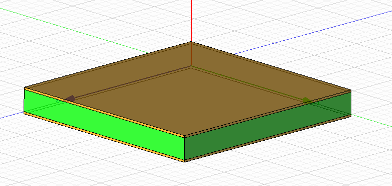
The Question
A recent homework problem had us derive the parallel plate capacitor1 equation for electrostatics. This gives the capacitance of a parallel plate structure in terms of the plate area, distance between the plates and relative permittivity. The equation for this situation is:
$ C = \epsilon_{R}\epsilon_{0}\frac{A}{d} $
After solving this problem for the analytical solution, I was curious to see how closely the result matched a 3D field solver. Using the Capacitance Extraction mode in Cadence 3D Workbench, I designed a parametric model of the parallel plate capacitor with variable edge length, distance and dielectric constant (See image above for the model). Dk 2 was varied but the complex component (dissipation factor) was set to zero to ignore any dielectric losses. The edges were swept at lengths of 0.1 inch, 1 inch and 10 inch. The distance was swept with values of 1mil, 10mil and 100mil. Finally, the dielectric constant was swept with values of 1, 10 and 100. This resulted in 27 unique cases, and the analytical result was compared to the extracted result in each case.
Figure 1. Data comparing parallel plate capacitor simulation to equation.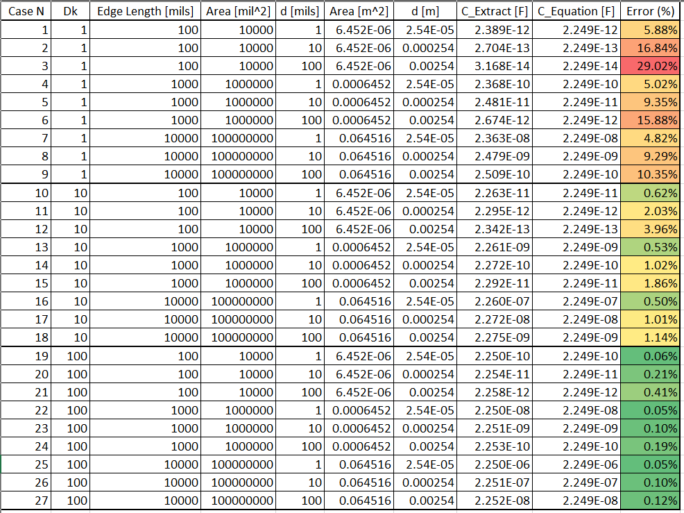
Results Analysis
There are two interesting takeaways from the results. First, we see much higher error when the area is not significantly larger than the dielectric height. This is expected because the field solver will correctly solve the fringe fields along the edges of the structure, while the equation is only valid when $A >> d$. These fringe fields result in a computed capacitance which is always higher than the equation-based formula. The reason we see more accuracy with smaller dielectric thickness is that the fringe fields do not extend very far laterally from the structure in that case.
The second major takeaway is that we see much better agreement between simulation and equation when the dielectric constant is higher. The better agreement here is likely due to the fact that the absolute value of the capacitance is much higher, therefore an error of a few $pF$ is still a smaller percentage variation.
If anyone's curious to play around with the 3D Workbench file, it's available here:
Update (Oct. 4, 2020)
I had a quick chance to investigate the electric field intensity vectors while varying the dielectric constant. Below are cutaway plots showing the electric field intensity within both the dielectric material and surrounding air. Note that the scale is kept the same on both plots for easier comparison.
Figure 2. Fringe electric field, $Dk = 1$.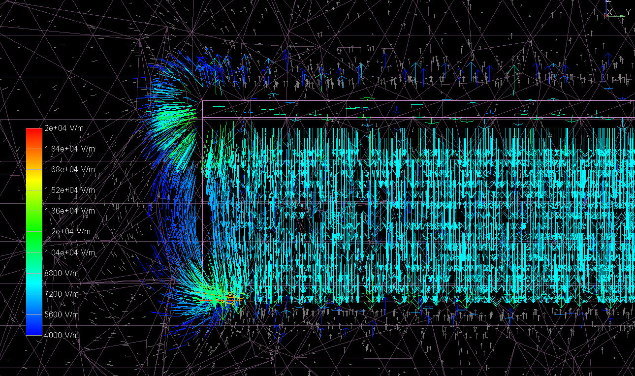
Figure 3. Fringe electric field, $Dk = 100$.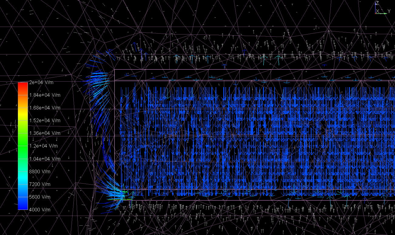
One interesting feature seen from this comparison is that the field intensity within the dielectric material is much stronger for lower Dk. This makes perfect sense; in reference 1, we see that the electric field magnitude can be represented using Gauss's Law3 as:
$ E = \frac{\sigma}{\epsilon} $
Thus, reducing Dk will increase the electric field intensity. The direction of the field can be seen as normal to the conductors, even wrapping around the conductor edges. Since the effective Dk at the edge is lower in Figure 2, the field intensity is higher out to a further distance. What are the practical implications of this characteristic? We know that in nearly all cases, lower Dk is better since we can use wider traces for a given dielectric thickness (resulting in lower skin effect losses).4 It also helps with crosstalk since there will be lower capacitive coupling. Lastly, since the flight time of a signal is inversely proportional to the square root of Dk, a lower Dk will result in a longer flight time (in $\frac{ps}{inch}$). This means that if you have to match two traces to within a certain flight time, the physical trace length mismatch is more forgiving with lower Dk material.
When would we want a higher Dk material? I can think of one very important situation: power and ground planes. We can improve the design of the power distribution network ( PDN ) with higher Dk material, as well as using the thinnest dielectric possible between these planes. In addition to increasing the capacitance of the PDN , this arrangement will also reduce the inductance which will help with ground bounce and extend the effective frequency range of the PDN .
So, what can be done to reduce fringing fields along the edges of PCBs? The 20H rule was once touted as a method of reducing these fields. I believe one of the origins of the 20H rule may be this5 set of guidelines (see the 7th bullet point). While this study did not look into the effects of the 20H rule , many authors consider the 20H rule to be a bit of a myth which has been confirmed by research.6 Whether or not the power planes are recessed, I have always considered an edge fence of ground vias to be an effective way to suppress fringe fields around a board. Sounds like a great topic for follow-up investigation!
Footnotes
Table of Contents
Related Engineering Insights
The Quickest Antenna Design of the Year
During a recent weekend, I found myself with some parts laying around which I …
Antenna Analysis from Ham Radio to PCBs
Has anyone else ever thought about why so many engineers are also active …
S-Parameters from a Neural Network
Continuing on the theme of using machine learning to speed up electromagnetic …
